Our services

At Pikotera, UAB, we design electronics devices and software for their control.

Having the know-how of data gathering from sensors grids, remote long-range (more than 8 km) data transfer, radio frequencies (RF) modules development and software design, as well as having created various devices acting independently, we provide with whole technical design R&D services for devices aimed to collect/transfer data or act according to remote commands.

Electronics engineering

Schematics design

Printed circuit boards design

Embedded software development

PCBA testing JIGs

Device operation analysis

Testing plan preparation

PCBA jig development and testing

Wireless data transfer solutions

Standard type communication (Wi-Fi, GSM, LTE)

Low energy standard type communication (LoRa, Bluetooth low energy)

Custom type comminication

User interfaces

Electronic devices and networks management (Windows, Android)

Collected data storage and customized reports

Data processing algorithms development

Research and development

Concept formulation
Proof of concept
R&D in electronics and mechatronics fields

Assistance in initial batch manufacturing

Arrangement with manufacturer of technical details
Optimization of design for manufacturing
Manufacturing tests development

WANT TO KNOW MORE?

Our projects

AbiliBalance

Electronics devices, Interactive gadgets

Lora wan

Wireless data gathering, IoT

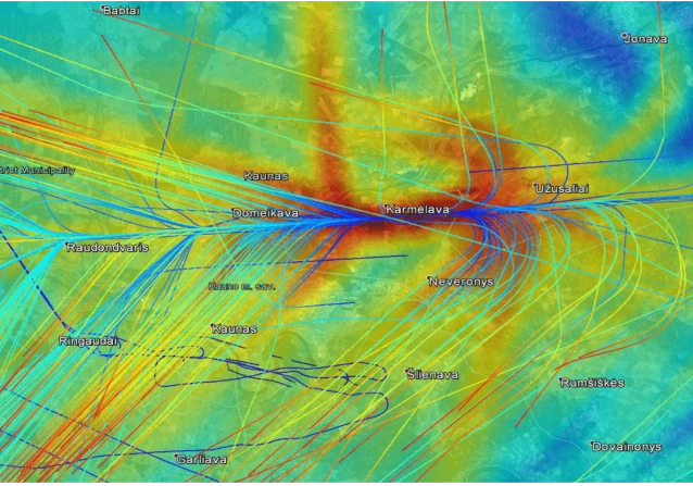
Sensors Integration, Data Augmentation, Visualization

Industry digitization, Industry 4.0

Industrial devices digitization, Industry 4.0

testing-fixture

PCBA testing fixtures

How we work

We are looking for long-term partnerships. While some companies are focusing on production or commercialization, we are willing to work closely and become their outsourced R&D department. Our clients come from various fields, often having an idea of a new device or improvement but not necessarily the technical knowledge. If needed, we provide with market-present solutions analysis and suggest the possibilities to implement an idea with currently available solutions.

In case the decision to design a new device or system is taken and functionalities list is prepared, the steps of product development provided by Pikotera are:

  1. Schematic files preparation;
  2. Printed circuit board (PCB) design;
  3. Embedded firmware development;
  4. Prototypes manufacturing, iterations;
  5. Prototypes testing;
  6. Software development (C#, Java, ROS for Windows, Linux or Android);
  7. Preparation for CE marking tests.
  8. Constructions/casings design.

In case more services are needed, we collaborate with partners for mechanical design, production and other services. Our goal is to help bringing the product, from an idea all the way to the ready-for-market state.

Latest news

New address

Pikotera is moving to even a greater location in Kaunas center! We are thankful to all our partners in „Vilko teritorija“ and around, who helped us learning and growing together. You will always be welcome in our new office in Laisvės al. 59, LT-44305 Kaunas, whenether passing by, for a cup of coffee or to discuss some great ideas 😊 We believe this new address is convenient for everyone to visit us. See you there!

Our new webpage

We are proud to present our new webpage which has been designed with an aim to present our services in simple and easy understandable way. We hope that this will save our customers time in searching information and contacting for needed solutions design.


Base for development and manufacturing

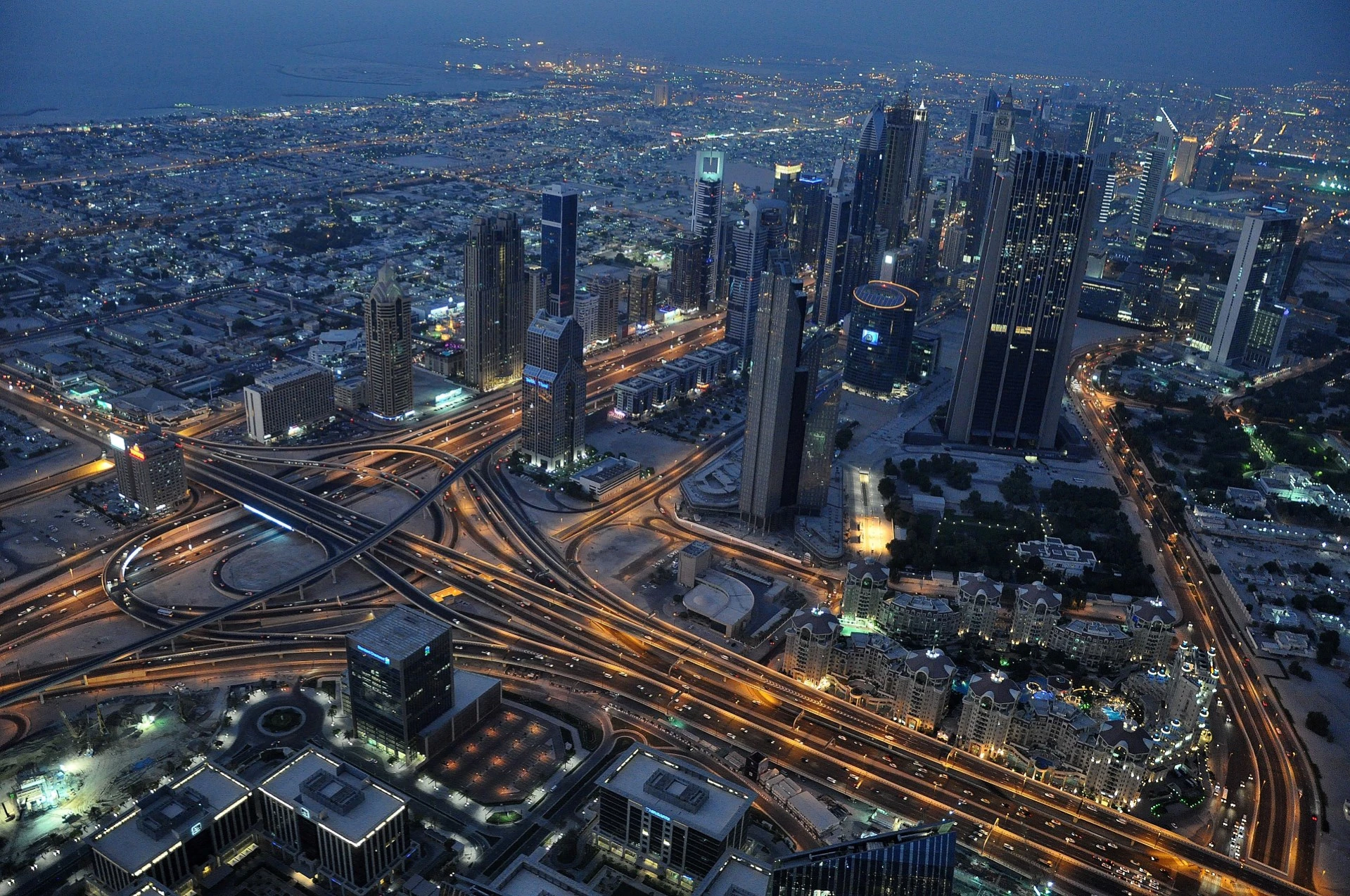
Lithuania is the perfect base for your manufacturing – both now, and as you grow. With a labour market that is 1.5 times less saturated than the CEE average, competitive labour costs, and a ready pipeline of highly qualified engineering talent, Lithuania has everything you need to scale your operations rapidly. Find out more in the Manufacturing Landscape of Lithuania report. Don't miss out – download your copy today!


Contact

For any general inquiries, please fill in the following contact form.

Email: info@pikotera.com